-
Notifications
You must be signed in to change notification settings - Fork 426
GL300 Main board
Function
Variants
Parts
Programming
External interfaces
Service interfaces
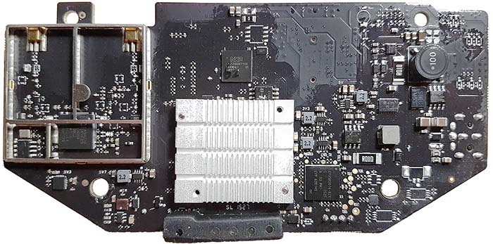
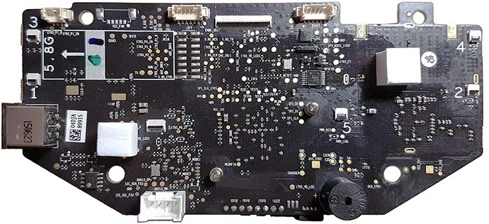
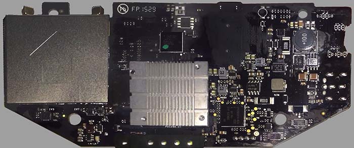
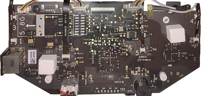
Board view
Schematics
The GL300 radio transmitter contains all vital elements on one board. The board is responsible of reading state of control sticks and switches, doing proper ADC conversion, then transmitting the control signal. But it also receives the Lightbridge video signal and telemetry from the drone, transcodes it and provides USB interface for reading the data and reconfiguring the drone from a mobile device.
There are 3 variants of GL300 controller used in P3X/P3S products, and additional variants for P4. Very similar boards are also used in GL658 remote controllers.
| Marking | Overview |
|---|---|
| GL300A | Used in first revisions of P3X and P3S. Requires video transcoder on the USB board. |
| GL300B | Update for later P3X and P3S drones; video transcoding was moved to a chip within the board, and newer USB controller was used. |
| GL300C | Came out with P4, but also used for new P3X and P3S drones since. |
| GL300E | Used in P4P. |
Variants of the board itself:
| Marking | Overview |
|---|---|
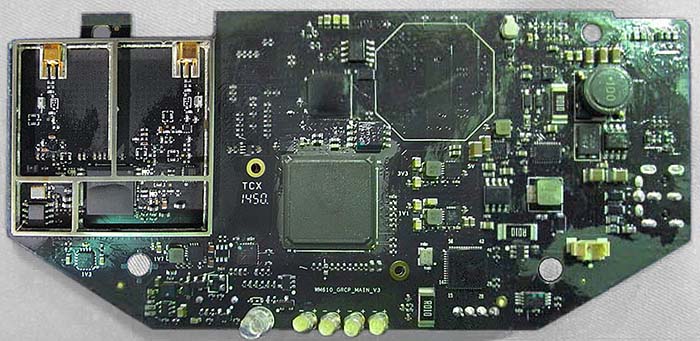
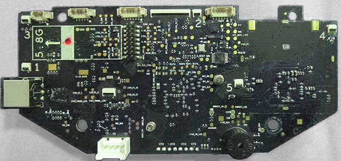
| WM610_GRCP_MAIN_V3 | Mostly used in GL658 Inspire controller; some evidence suggests that board was also used in early GL300A, but only this Altera V version. |
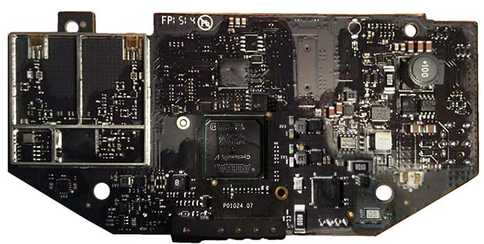
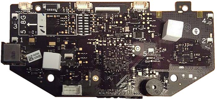
| P01024.07 | The usual GL300A board. |
| P01298.01 | Board used in GL300B, USB controller has changed and power estimation hardware was added. |
| P01298.05 | Board introduced in GL300C, but also found in newer GL300B. A switch in Lightbridge implementation was made from FPGA to ASIC chip, and NXP micro-controller was switched to lower model. Since 3 BGA chips were replaced by LQFP packages, this version should be much easier to repair at home. |
| P01298.08 | Late GL300C board. |
| Marking | Amt. | Pkg. | Function | Specification |
|---|---|---|---|---|
| Altera Cyclone V 5CEFA4U19I7 | 1 | 484-ball UFBGA | FPGA; Cyclone V E model 5CEA4, Ultra Fineline 484 pin BGA package, temp. range -40 to 100 deg C | description |
| NXP LPC1765 | 1 | Either LPC1765 or LPC1768; Cortex-M3 microcontroller | description | |
| CY7C68013 | 1 | High-Speed USB Peripheral Controller | ||
| C9257 TI144W 2265 | 1 | markings read error? | ||
| NS S58810 17YC1 4H1 | 1 | National Semiconductor logo; markings read error? | ||
| HYDZ | 1 | Piezoelectronic Buzzer |
| Marking | Amt. | Pkg. | Function | Specification |
|---|---|---|---|---|
| Altera Cyclone V 5CEFA4U19I7 | 1 | 484-ball UFBGA | FPGA; Cyclone V E model 5CEA4, Ultra Fineline 484 pin BGA package, temp. range -40 to 100 deg C | description |
| 25Q128A | 1 | 8-pin 4x5 SOP | Serial flash storing FPGA bitstream | |
| NXP LPC1765FET100 8AK902.1 09 ZSD1513A | 1 | Cortex-M3 microcontroller | description | |
| CYUSB2014-BZX C 1525 A 33 PHI CYP 620145 | 1 | SuperSpeed USB Controller | description | |
| Analog Devices AD9363 B8CZ | 1 | RF Agile Transceiver | description | |
| S86C M55 | 1 | |||
| AEUF | 4 | Buck converter | ||
| PA 5QA | 1 | 3x3 UDFN/WSON | Mini Linear Regultor; part used is DI AP7361ADJ, but it could also be TI TPS7A16 | DI datasheet TI description |
| C 5A AS | 1 | 8-lead | Atmel ATSHA204 CryptoAuthentication | |
| HYDZ | 1 | Piezoelectronic Buzzer |
| Marking | Amt. | Pkg. | Function | Specification |
|---|---|---|---|---|
| Artosyn AR8003 CAF202 1542 | 1 | RF transceiver | ||
| Artosyn AR8001 549P501N | 1 | Video encoder | ||
| NXP LPC1549JBD100 SCA352.1 30 ZSD15452A | 1 | Motion Control 32-bit Microcontroller based on ARM Cortex-M3 | description | |
| CYUSB2014-BZX C 1543 A 33 PHI CYP 635498 squareC | 1 | SuperSpeed USB Controller | description | |
| CW2015CWAD | 1 | power estimating | description datasheet | |
| S86C M57 | 1 | |||
| AEUF | 1 |
| Chips | Firmware | Description |
|---|---|---|
| ? | m0605 | Unknown; included in C1 FW packages |
| NXP LPC1765 | m1400 | Radio controller i/o processor in GL300a/b |
| NXP LPC1549 | m1401 | Radio controller i/o processor in GL300c |
| Cypress CYUSB2014 | m1601 | Lightbridge technology data serializer |
| Cypress CY7C68013 | m1600 | Lightbridge technology data serializer |
| FPGA | m2003 | Lightbridge 2 communication FPGA hardware model |
| FPGA | m2002 | Lightbridge communication FPGA hardware model |
| FPGA | m2001 | Lightbridge communication FPGA hardware model |
| FPGA | m2000 | Lightbridge communication FPGA hardware model |
Connectors on the board are:
| Marking | Overview |
|---|---|
| TODO |
Some of RC button combinations have special functions. Note that Cam Settings Dial wheel can not only be rotated, but also pressed. Location of each button can be found in the official manual.
| Combination | Overview |
|---|---|
| when RC is off, hold: C1, C2, Vid Record, Cam Settings Dial buttons simultaneously, while turning it on | Failsafe boot mode, for emergency firmware update. It worked if the status LED turned blue. |
| when RC is off, hold: C1, Shutter buttons simultaneously, while turning it on | Unknown mode. It worked if the status LED turned blue. |
| when RC is on, hold: C1, C2, Shutter buttons simultaneously, while turning it off | Restore factory settings. It worked if a special quick audio queue was played. |
| when RC is on, hold: C1, C2, Vid Record buttons simultaneously, until beep (dash-dot-dot) | Special mode selection; lasts only ~3 seconds. From there you can enter RC Linking Mode by pressing Cam Settings Dial button. Cancel by pressing playback button. |
The following service pads exist on this board:
| Marking | Overview |
|---|---|
| PMODE0 | Boot mode selector bit 0 for Cypress chip |
| PMODE1 | Boot mode selector bit 1 for Cypress chip |
| PMODE2 | Boot mode selector bit 2 for Cypress chip |
| 1765_RX | receive for Cypress chip |
| 1765_TX | transmit for Cypress chip |
| TODO |
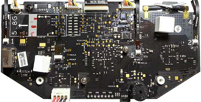
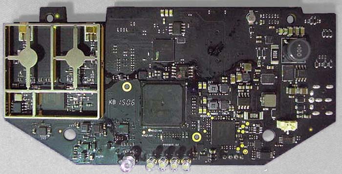
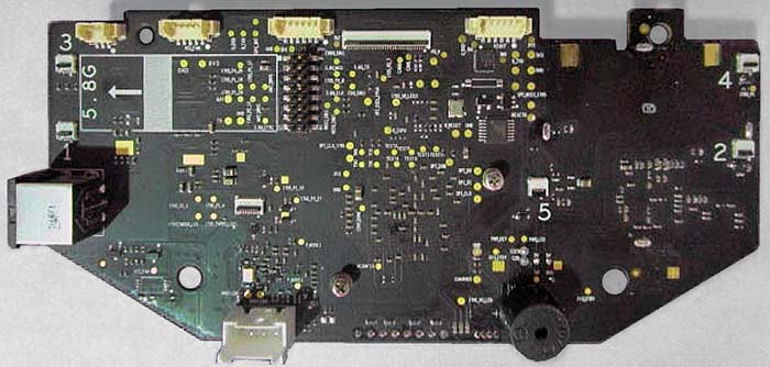
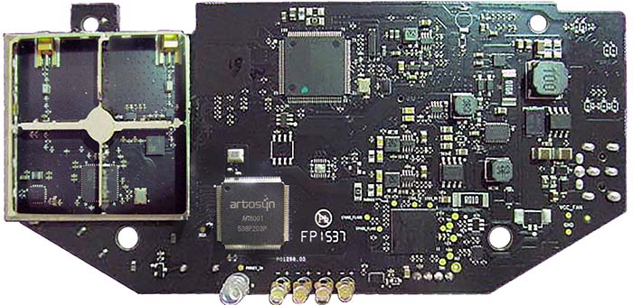
Top of a WM610_GRCP_MAIN_V3 board from early P3X:
Bottom of the WM610_GRCP_MAIN_V3 board:
Top of a P01024.07 board:
Bottom of the P01024.07 board:
Top of a P01298.01 board:
Bottom of the P01298.01 board:
Top of another P01298.01 board:
Bottom of an unknown GL300A board:
Bottom of another unknown GL300A board:
Top of an unknown P01298.0? (<05) board from P3X:
Bottom of the unknown P01298.0? board:
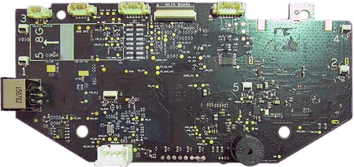
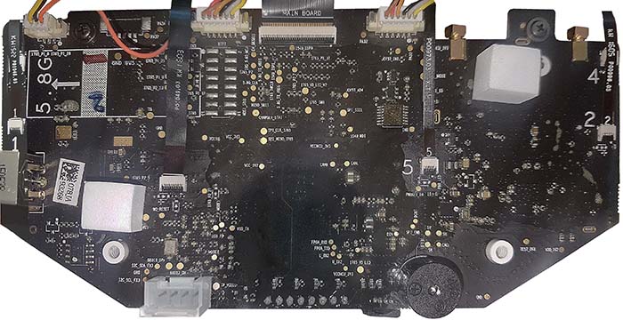
Top of a P01298.05 board from P4:
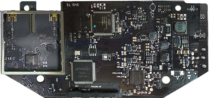
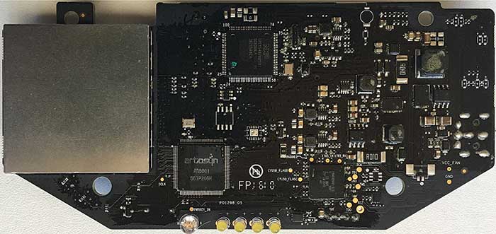
Bottom of the P01298.05 board:
Top of another P01298.05 board from P4:
Bottom of an unknown GL300C board:
Top of yet another P01298.05 board, with FFC connector damage:
Bottom of the P01298.05 board:
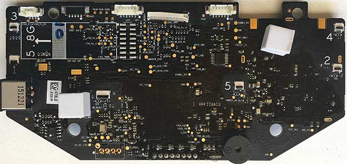
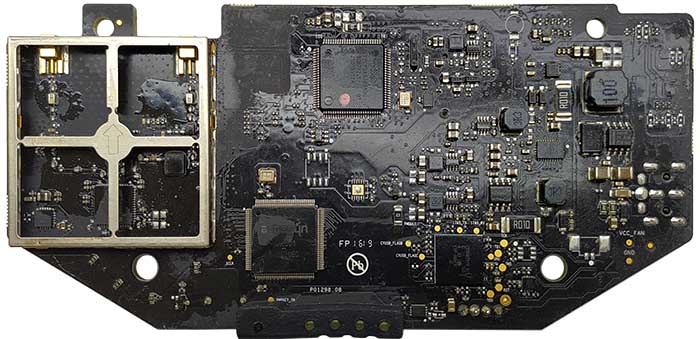
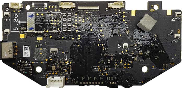
Top of P01298.08 board:
Bottom of the P01298.08 board:
No schematics available.
This page is created by drone enthusiasts for drone enthusiasts.
If you see a mistake, or you know more about specific subject, or you see an area for improvement for the wiki - create an issue in this project and attach your patch (or describe the change you propose).
